FPGAs and Retro Gaming: How Programmable Chips Are Replacing Your Old Consoles
The Problem With Emulation (And Why People Keep Yelling About It)

If you have spent any time in retro gaming communities, you have encountered The Argument. Someone posts a screenshot of their MiSTer FPGA setup. Someone else says emulation on a Raspberry Pi does the same thing. Then a third person materializes to explain that neither is acceptable and you need to play on original hardware connected to a CRT or you are not really experiencing the game. Three hours later, everyone is angry and nobody has actually played any games.
The truth is more interesting than the argument. Software emulation and FPGA recreation are solving the same problem in fundamentally different ways, and understanding the difference requires looking at how a retro console actually works. Not at a surface level, but at the level of electrons and clock cycles. It is genuinely fascinating stuff, and it explains why a chip you can reprogram is quietly becoming the most important technology in retro gaming preservation.
What Your SNES Is Actually Doing
Let us use the Super Nintendo as our example, because it is one of the most beloved and well-documented consoles ever made. When you think of the SNES, you probably think of it as a single machine that runs games. In reality, it is a collection of independent processors all running simultaneously, each handling a different job, all talking to each other through shared memory and bus lines.
The Ricoh 5A22 handles the main CPU duties, running game logic, managing controller input, and orchestrating everything else. But the visuals are handled by two entirely separate chips called PPU1 and PPU2, the Picture Processing Units. These are dedicated graphics processors that manage backgrounds, sprites, color math, and that famous Mode 7 rotation effect that made F-Zero and Super Mario Kart look so impressive. Meanwhile, the audio system runs on its own completely isolated subsystem: a Sony SPC700 processor paired with an S-DSP chip, operating at its own clock speed with its own dedicated memory. The CPU cannot even access the audio memory directly: it has to send data through a set of four shared I/O ports, like passing notes under a door.
All of these chips run in parallel. At any given moment, the CPU might be calculating enemy positions, the PPU is drawing scanline 147 of the current frame, and the audio processor is mixing channel 6 of the background music. They are not taking turns. They are all working at the same time, on their own clocks, producing results that combine into what you see and hear on screen.
Why This Matters for Emulation
Software emulation has to simulate all of this on a fundamentally different kind of machine. Your PC or phone has a single CPU (or a few cores) that executes instructions one after another. To emulate a SNES, the emulator has to fake the parallel operation of all those separate chips by rapidly switching between simulating each one, a little bit at a time.

A good SNES emulator will run a few cycles of the CPU, then switch to running a few cycles of the PPU, then handle some audio processing, then check if a DMA transfer needs to happen, then go back to the CPU. It is doing this thousands of times per frame, carefully tracking how many cycles each component has consumed to keep everything in sync. This approach works remarkably well, emulators like bsnes and higan achieve extraordinary accuracy, but it is fundamentally a sequential approximation of a parallel system.
The consequences show up in edge cases. When the SNES CPU and PPU interact within the same scanline, the exact timing of bus access and register writes matters down to the individual clock cycle. Games like Air Strike Patrol use a mid-scanline technique to change the background scroll position partway through drawing a line, creating a pseudo-3D shadow effect on the ground. If the emulator's cycle timing is off by even a small amount, the effect breaks. Achieving this level of accuracy in software requires simulating the hardware at a granular, cycle-by-cycle level, which demands significantly more processing power than a looser approximation would need.
Enter the FPGA
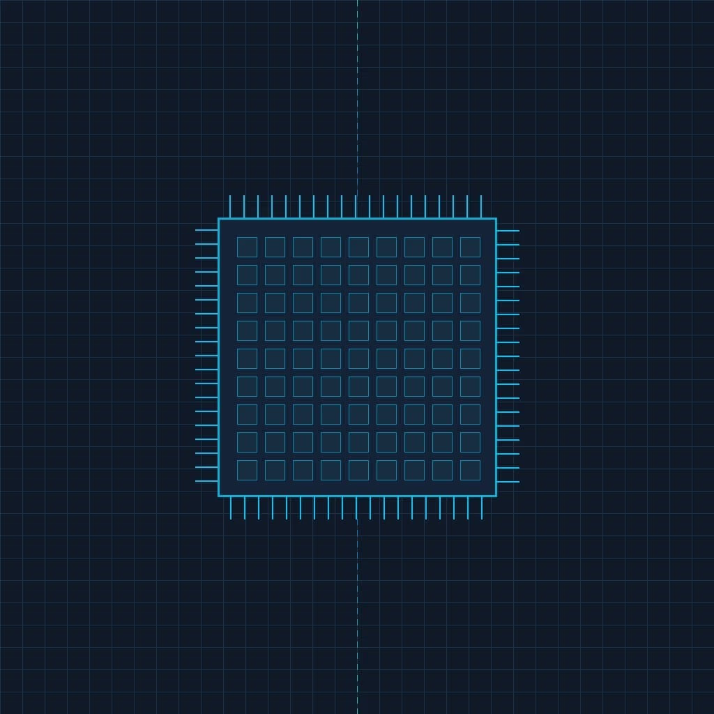
An FPGA, Field-Programmable Gate Array, is a chip made of configurable logic blocks that can be wired together to create arbitrary digital circuits. Instead of running software that pretends to be a SNES, an FPGA physically becomes the equivalent digital logic. The parallel operation is not simulated: it actually happens. The CPU logic runs on one set of logic blocks, the PPU runs on another set, and the audio processor runs on yet another, all clocked and connected just like the original silicon.
To understand how this works, you need to know about the building blocks inside an FPGA. The two most fundamental are lookup tables and flip-flops. A lookup table, or LUT, is a tiny chunk of memory that can implement any logical function of its inputs. A modern FPGA uses 6-input LUTs, meaning each one can take six binary inputs and produce any output you want, it has been pre-loaded with the correct answer for every possible combination of inputs, all 64 of them. Need an AND gate? A LUT can do that. Need a complex priority encoder? Also a LUT (or a few of them chained together). These are the fundamental computing elements, the equivalent of transistors in a custom chip.
Flip-flops are the memory elements. Each one stores a single bit of information and updates its value on the edge of a clock signal. Every register in the original SNES hardware, the CPU's accumulator, the PPU's scroll position counters, the audio DSP's envelope state, is recreated as a collection of flip-flops in the FPGA. When the clock ticks, all of these flip-flops update simultaneously, just like they did in the original hardware.
Building a Console in Programmable Logic
When someone writes an FPGA core for the SNES, they are describing the behavior of each original chip using a hardware description language like Verilog or VHDL. This is not programming in the traditional sense: it is closer to designing a circuit. You are specifying what logic connects to what, what happens on each clock edge, and how data flows between components.
The FPGA development tools take this description and figure out how to map it onto the physical resources of the chip. The CPU's ALU operations get assigned to specific LUTs. The PPU's tile lookup logic gets its own cluster of LUTs. The audio DSP's sample interpolation gets mapped to the FPGA's dedicated DSP blocks, hardwired multiplier units that can do the multiply-accumulate operations needed for audio mixing without consuming general-purpose logic.
The result is a chip that contains the functional equivalent of all the SNES's processors, running in true parallel, updating on real clock edges. When the PPU needs to read a tile from VRAM while the CPU is simultaneously executing an instruction, both of those things actually happen at the same time, mediated by bus arbitration logic that matches the original hardware's priority scheme, which gives HDMA (horizontal DMA) the highest priority, then general DMA, then the CPU.
The Clock Problem
One of the trickiest aspects of recreating retro hardware in an FPGA is dealing with multiple clock domains. The SNES master clock runs at 21.477 MHz. The CPU divides this down and typically operates at around 2.68 MHz (though the exact speed varies depending on which memory region is being accessed: the SNES dynamically adjusts CPU speed based on how fast the target memory can respond). The PPU operates at the full master clock rate. The audio subsystem runs on a completely independent 2.048 MHz clock.
In the original hardware, these different clock domains create a genuine engineering challenge. When two circuits running on different clocks need to exchange data, there is a risk of something called metastability, a flip-flop catching a signal right at the moment it is changing, resulting in an output that is neither a clean 0 nor a clean 1 but an indeterminate voltage that can propagate errors through the system.
The original SNES engineers solved this with synchronization circuits, and FPGA core developers have to do the same thing. The standard approach is a two-stage synchronizer: the incoming signal passes through two flip-flops clocked by the receiving domain before it is used. This does not eliminate metastability, but it reduces the probability to astronomically small levels. FPGA cores for the SNES use these synchronizers at every boundary between clock domains, just as the original hardware did.
Modern FPGAs include PLLs (Phase-Locked Loops) that can synthesize precise clock frequencies from a single input crystal. A MiSTer FPGA core for the SNES will use PLLs to generate the exact master clock frequency and derive all other clocks from it, matching the original timing to a degree that software emulation can only approximate through careful cycle counting.
Enhancement Chips: Where Things Get Really Interesting
The SNES had a trick up its sleeve that made it one of the most versatile consoles of its generation: cartridge-based enhancement chips. Because the cartridge slot had direct access to the CPU bus, game developers could put additional processors inside the cartridge itself, extending the console's capabilities on a per-game basis.
The most famous of these is the Super FX chip, which gave the SNES rudimentary 3D polygon capabilities. Star Fox, Stunt Race FX, and Doom all used the Super FX to render 3D graphics that the base SNES hardware could never have produced. The SA-1 chip was essentially a second, faster CPU that ran at 10.74 MHz, four times the speed of the main CPU, and was used in games like Kirby Super Star and Super Mario RPG to handle complex game logic. The DSP-1 provided fixed-point math acceleration for games like Super Mario Kart and Pilotwings.
For software emulation, each enhancement chip is another processor that needs to be simulated, adding complexity and CPU overhead. For FPGA recreation, each enhancement chip is another block of logic that runs in true parallel with everything else. The Super FX core runs on its own set of LUTs, doing its polygon math at the same time the main CPU handles game logic and the PPU draws the screen. This is exactly how the original hardware worked: the Super FX chip was literally a separate processor running simultaneously inside the cartridge.
This is where FPGAs have a structural advantage that software emulation can never fully match. Adding another parallel processor to an FPGA just means using more of the chip's available resources. Adding another parallel processor to a software emulator means the single-threaded simulation loop has to interleave yet another set of cycle-accurate state updates, making the timing juggling act even more complex.
The MiSTer Platform
The MiSTer FPGA project has become the de facto standard for FPGA-based retro gaming. It is built around the Terasic DE10-Nano board, which features an Intel (formerly Altera) Cyclone V FPGA. The specific chip, the 5CSEBA6U23I7, provides over 110,000 adaptive logic modules (ALMs, Intel's term for their LUT-plus-flip-flop units), 553 blocks of on-chip memory, and 112 DSP blocks.
To put those numbers in context: a complete SNES implementation, including CPU, both PPUs, audio subsystem, and several enhancement chips, uses a fraction of the Cyclone V's available resources. This is why MiSTer can run cores for systems as complex as the PlayStation and even the Nintendo 64: there is simply enough programmable logic on the chip to instantiate all the digital circuitry those consoles contained.
The MiSTer also adds what the original consoles did not have: an ARM processor running Linux that handles the user interface, file management, and configuration. Your ROM files live on an SD card or USB drive, and the Linux system loads them into SDRAM that the FPGA core accesses as if it were a cartridge ROM or disc drive. This is one of the few compromises involved, the original consoles read from ROM chips or optical media, while MiSTer reads from SDRAM, but the access patterns and timing are carefully matched to the original hardware's behavior.
FPGA vs. Emulation: The Real Tradeoffs
The FPGA versus emulation debate is often framed as FPGA being "better," but the reality is more nuanced than that.
FPGAs excel at timing accuracy and parallel execution. For systems where cycle-exact behavior matters, where games exploit hardware quirks, rely on precise timing windows, or interact with enhancement chips in complex ways, an FPGA implementation is architecturally better suited to the task. The accuracy comes from the structure of the implementation, not from the raw power of the host hardware.
Software emulation excels at flexibility, accessibility, and convenience. A software emulator can run on hardware you already own. It can offer features like save states, rewinding, shader effects, and netplay that require access to the emulated system's state in ways that hardware recreation does not naturally support (though MiSTer has added many of these features over time). Emulators are easier to update, easier to distribute, and easier to develop, writing C++ is more accessible than writing Verilog.
The accuracy gap has also narrowed significantly. Modern cycle-accurate emulators like bsnes achieve compatibility rates that are, for practical purposes, identical to FPGA cores. The remaining differences are in edge cases that affect a handful of games, and even those gaps are closing as both FPGA cores and software emulators continue to improve.
For most people playing most games, both approaches deliver excellent results. The choice between them is more about values and priorities, whether you care more about the philosophical purity of hardware recreation, the practical flexibility of software, or the specific features each platform offers, than about a meaningful difference in the experience of playing Super Mario World.
Why It Matters for Preservation
Here is where FPGA technology becomes genuinely important beyond the hobbyist debate. Original retro gaming hardware is dying. Capacitors leak, custom chips fail, cartridge connectors corrode, and the specialized components that made each console unique are not being manufactured anymore. Every year, the pool of working original hardware shrinks, and it is never coming back.
Software emulation preserves the software: the games themselves. FPGA recreation preserves the hardware behavior: the specific way those games were meant to run, down to the timing quirks and analog output characteristics that defined the experience. Both forms of preservation are valuable, and they complement each other. The emulator developers and the FPGA core developers often share research, documentation, and test results, each approach informing and improving the other.
The FPGA community has also become an important force in documenting how original hardware actually worked. Writing an FPGA core for a console requires understanding that console's hardware at an intimate level, every register, every timing constraint, every undocumented behavior that games might depend on. This process generates detailed technical knowledge that benefits the entire preservation ecosystem, including software emulation.
What Comes Next
FPGA technology is still evolving rapidly. The current generation of affordable FPGAs used in devices like MiSTer is powerful enough to handle most 16-bit and many 32-bit systems, but more complex consoles like the Saturn (with its notoriously complicated multi-processor architecture) and the N64 push the boundaries of what current hardware can achieve. Larger, more capable FPGAs exist, but at higher price points that strain the budget-conscious nature of the hobby.
The Analogue Pocket and Analogue Duo have demonstrated that FPGA-based retro gaming can be packaged into polished consumer products that do not require any technical knowledge to use. As the market for these products grows, so does the incentive for manufacturers to invest in larger FPGAs and more sophisticated core development.
The most exciting possibility is one that the retro gaming community has been gradually working toward: a comprehensive, hardware-accurate digital archive of every major gaming platform, playable on modern hardware with the timing fidelity of the original silicon. FPGAs are not the only path to that goal, but they are a uniquely powerful one, and the community building these cores is doing some of the most impressive engineering work happening anywhere in gaming today. Even if you never buy a MiSTer or an Analogue Pocket, the work being done on these platforms is making retro gaming better for everyone.